Photovoltaics
Accelerated material development and testing of materials for efficient photovoltaic cells
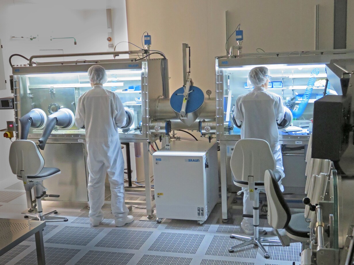
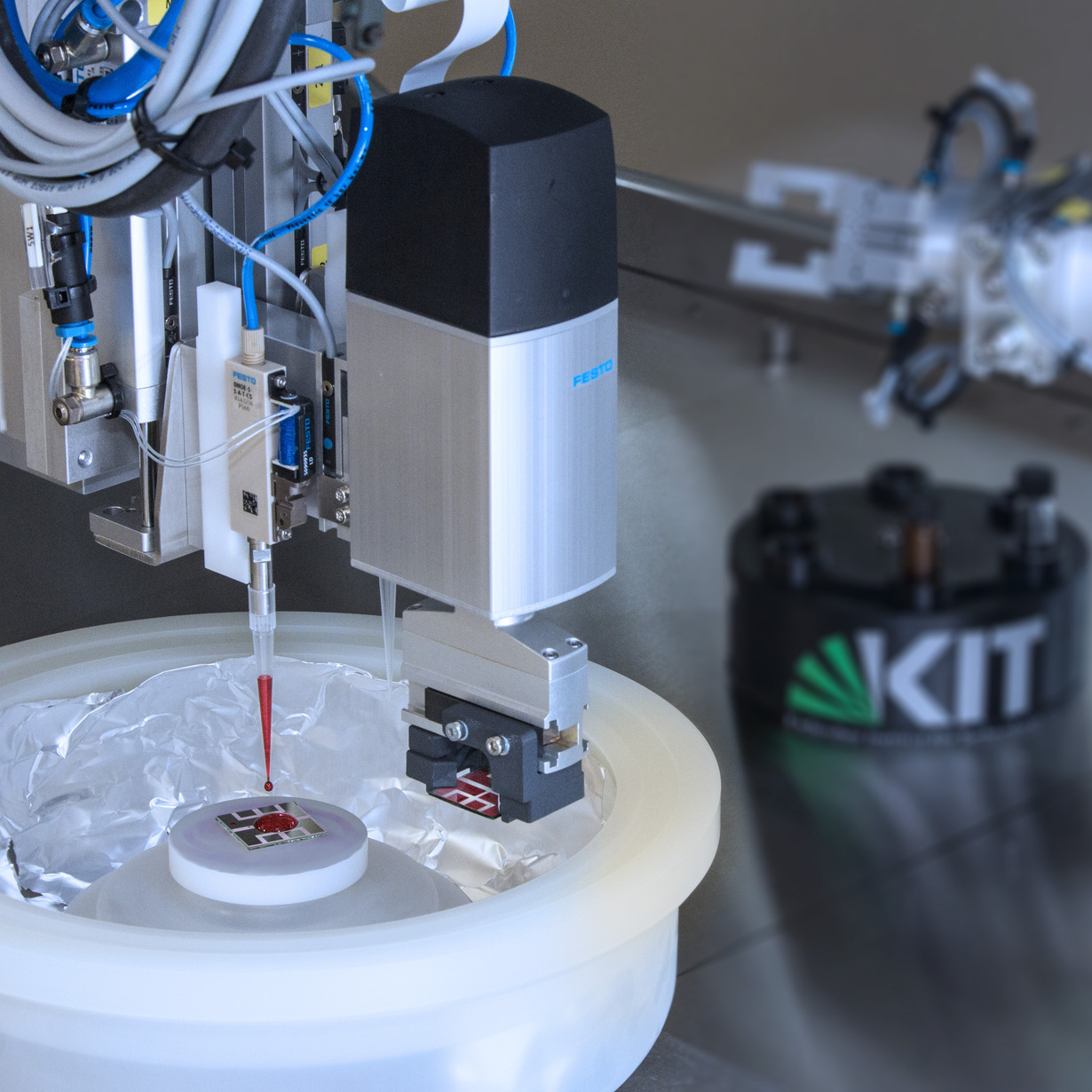
The research idea behind the Energy Materials Acceleration Platform (E-MAP) is the automated processing and characterisation of energy materials from the fields of photovoltaics, light emission, optoelectronics and other thin-film applications. It consists of three fully integrated process sections. In the first section, semiconductor inks are synthesised using combinatorial microfluidics and pipetting. So far, the focus has been on colloidal organic semiconductor systems, which are used for the environmentally friendly processing of organic solar cells. This includes the characterisation of the inks using UV-VIS spectrometry and dynamic light scattering. The second section involves the automated deposition of thin films using spin coating. Extensions with regard to substrate preparation and post-treatment as well as alternative deposition methods are currently being planned. The third section consists of six modular bays in which suitable characterisation techniques can be installed according to current requirements. Modules for photoluminescence, charge carrier mobility and light absorption measurements are currently under construction.